 |
 |
|
|
| Changed: |
<
< |
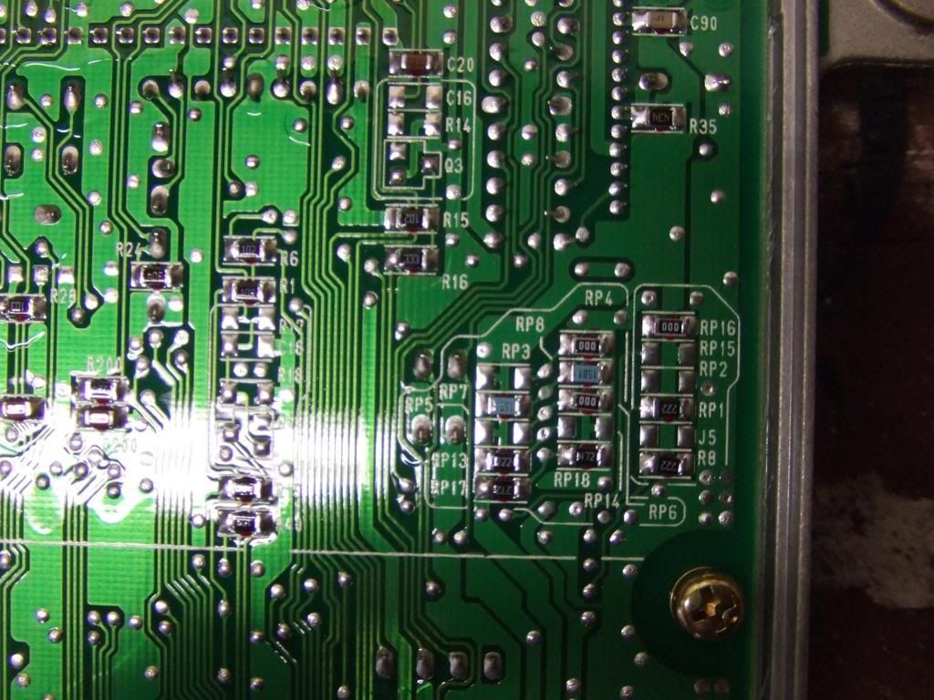
Lastly if you are wanting to convert Auto to manual remove the resistor RP18 '472' on the back and replace it with a 1.4K or 1.5K resistor. Shown in bottom right of the picture.
| >
> |
Lastly if you are wanting to convert Auto to manual remove the resistor RP18 '472' on the back and replace it with a jumper wire. Also remove RP17 and leave it open. A/T resistor layout shown in bottom right of the picture. |
|
|
| Changed: |
<
< |
Add C49 & C50 and C91 & C92 on back
| >
> |
Add C49 & C50 and C92 on back. C91 is on the front by the latch
|
| Added: |
>
> |
The Above picture is untrue, many A/T boards need the latch and the socket. As there are different variants of the JDM P30 Board
|
| Changed: |
<
< |
For RTP/Datalogging w/ Crome remove J4 on front.
| >
> |
For RTP/Datalogging w/ Crome remove J4 on front. (J4 is a 000 resistor)
|
| Added: |
>
> |
Lastly if you are wanting to convert Auto to manual remove the resistor RP18 '472' on the back and replace it with a 1.4K or 1.5K resistor. Shown in bottom right of the picture.
 |
|
|
| Changed: |
<
< |
C49 & C50 --> .004UF
| >
> |
C49 & C50 --> .004UF (Digikey part number 399-1230-1-nd )
|
| Changed: |
<
< |
C91 & C92 --> .00001UF
| >
> |
C91 & C92 --> .00001UF ( digikey Part Number 399-1192-1-nd ) |
|
|
| Changed: |
<
< |
Add the 74hc373 SMD chip.
| >
> |
Add the 74hc373 SMD chip. (MFG part# SN74HC373NSR, Digi-Key Part Number 296-8310-1-ND) |
|
|
| Added: |
>
> |
%META:TOPICINFO{author="LegoZ81" date="1110569760" format="1.0" version="1.1"}%
%META:TOPICPARENT{name="IntroductionToECUChipping"}%
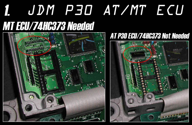
You will need bridge J1 on the back of the ECU.
 Add C49 & C50 and C91 & C92 on back
C49 & C50 --> .004UF
C91 & C92 --> .00001UF
Add C49 & C50 and C91 & C92 on back
C49 & C50 --> .004UF
C91 & C92 --> .00001UF
 Add the 74hc373 SMD chip.
 Add a 29C256 eprom with bin written to it.
For RTP/Datalogging w/ Crome remove J4 on front.
Solder in a 4 pin header (snappable header pins 1x40 work GREAT for this and are VERY cheap)
All info is from the following threads:
http://forum.pgmfi.org/viewtopic.php?t=3112&highlight=chipping+jdm+computers
Special thanks to all the contributors of the above thread and katman for doing the pics in
the first place... We love you katman :)
http://forum.pgmfi.org/viewtopic.php?t=4005&highlight=chipping+jdm+computers
Thanks to infotechplus for pics and info on C49,C50,C91,C92
Add a 29C256 eprom with bin written to it.
For RTP/Datalogging w/ Crome remove J4 on front.
Solder in a 4 pin header (snappable header pins 1x40 work GREAT for this and are VERY cheap)
All info is from the following threads:
http://forum.pgmfi.org/viewtopic.php?t=3112&highlight=chipping+jdm+computers
Special thanks to all the contributors of the above thread and katman for doing the pics in
the first place... We love you katman :)
http://forum.pgmfi.org/viewtopic.php?t=4005&highlight=chipping+jdm+computers
Thanks to infotechplus for pics and info on C49,C50,C91,C92 |
|
Copyright © 2002-present by the contributing authors. All material on this collaboration platform is the property of the
contributing authors, and is covered by the Non-Commercial Share-Alike License unless explicitly stated otherwise. |
|